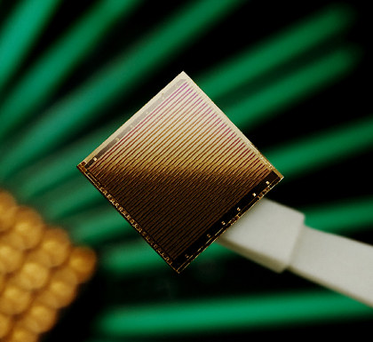
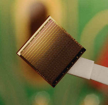
Dai ricercatori di Intel e dall'Università californiana di Santa Barbara è arrivato l'annuncio della realizzazione del primo chip al mondo in tecnologia Hybrid Silicon Laser. Utilizzando quelle che sono le tecniche standard per la realizzazione dei chip in silicio e ricorrendo ad uno speciale semiconduttore ovvero l'Indium Phosphide (è una miscela di indio e fosforo, ndr) il colosso americano della microelettronica è riuscito nell'intento di produrre a basso costo un chip che può cambiare radicalmente la storia dei dispositivi.
[Immagine ad alta risoluzione]
La soluzione è detta ibrida poichè è in grado di combinare le proprietà irradianti dell'Indium Phosphide con quelle rifrattive del silicio: in tal modo all'applicazione di una tensione (e alla conseguente generazione di un campo elettrico, ndr) l'Indium Phosphide genera un fascio di luce (laser) che viene instradato nella struttura di silicio che agisce come una guida d'onda, supportando la propagazione del segnale luminoso.
[Immagine ad alta risoluzione]
L'annuncio di Intel è d'importanza rilevante poichè lega la trasmissione dei dati nello stato di radiazioni luminose alla economica e consolidata tecnologia produttiva del silicio: ciò consentirà in un futuro, a questo punto nemmeno troppo lontano, di produrre a basso costo chip aventi requisiti in termini di ampiezza di banda e frequenza operativa significativamente superiori a quelli garantiti dalle odierne soluzioni.

SANTA CLARA, Calif., Sept. 18, 2006 Researchers from Intel Corporation and the University of California, Santa Barbara (UCSB) have built the worlds first electrically powered Hybrid Silicon Laser using standard silicon manufacturing processes. This breakthrough addresses one of the last major barriers to producing low-cost, high-bandwidth silicon photonics devices for use inside and around future computers and data centers.
The researchers were able to combine the light-emitting properties of Indium Phosphide with the light-routing capabilities of silicon into a single hybrid chip. When voltage is applied, light generated in the Indium Phosphide enters the silicon waveguide to create a continuous laser beam that can be used to drive other silicon photonic devices. A laser based on silicon could drive wider use of photonics in computers because the cost can be greatly reduced by using high-volume silicon manufacturing techniques.
This could bring low-cost, terabit-level optical data pipes inside future computers and help make possible a new era of high-performance computing applications," said Mario Paniccia, director of Intels Photonics Technology Lab. "While still far from becoming a commercial product, we believe dozens, maybe even hundreds of hybrid silicon lasers could be integrated with other silicon photonic components onto a single silicon chip.
"Our research program with Intel highlights how industry and academia can work together to advance the state of science and technology," said John Bowers, a professor of electrical and computer engineering at UC Santa Barbara. By combining UCSBs expertise with Indium Phosphide and Intels silicon photonics expertise, we have demonstrated a novel laser structure based on a bonding method that can be used at the wafer-, partial-wafer or die-level, and could be a solution for large-scale optical integration onto a silicon platform. This marks the beginning of highly integrated silicon photonic chips that can be mass produced at low cost.
Technical Details
While widely used to mass produce affordable digital electronics today, silicon can also be used to route, detect, modulate and even amplify light, but not to effectively generate light. In contrast, Indium Phosphide-based lasers are commonly used today in telecommunications equipment. But the need to individually assemble and align them has made them too expensive to build in the high volumes and at the low costs needed by the PC industry.
The hybrid silicon laser involves a novel design employing Indium Phosphide-based material for light generation and amplification while using the silicon waveguide to contain and control the laser. The key to manufacturing the device is the use of a low-temperature, oxygen plasma -- an electrically charged oxygen gas -- to create a thin oxide layer (roughly 25 atoms thick) on the surfaces of both materials.
When heated and pressed together the oxide layer functions as a glass-glue fusing the two materials into a single chip. When voltage is applied, light generated in the Indium Phosphide-based material passes through the oxide glass-glue layer and into the silicon chips waveguide, where it is contained and controlled, creating a hybrid silicon laser. The design of the waveguide is critical to determining the performance and specific wavelength of the hybrid silicon laser. More information on the Hybrid Silicon Laser can be found at http://www.intel.com/research/platform/sp/hybridlaser.htm.
Todays announcement builds on Intels other accomplishments in its long-term research program to siliconize photonics using standard silicon manufacturing processes. In 2004, Intel researchers were the first to demonstrate a silicon-based optical modulator with a bandwidth in excess of 1GHz, nearly 50 times faster than previous demonstrations of modulation in silicon. In 2005, Intel researchers were the first to demonstrate that silicon could be used to amplify light using an external light source to produce a continuous wave laser-on-a-chip based on the Raman effect.
Bowers has worked with Indium Phosphide-based materials and lasers for more than 25 years. Currently his research is focused on developing novel optoelectronic devices with data rates as high as 160Gb/s and techniques to bond dissimilar materials together to create new devices with improved performance.
News Source: Intel Press Release
Links